Simultaneous production of differently doped areas on a solar cell using borosilicate glass
Abstract
Using a new process, both negatively and positively doped areas can be created on the back of the solar cell and the front of the solar cell can be sufficiently passivated in a single diffusion step. This approach is based on the application of a borosilicate glass layer and partial silicon nitride masking on the rear of the solar cell.
Advantages
- Three different types of doping in a single-step diffusion process (e.g. areas with higher and lower phosphorus doping levels as well as boron-doped areas)
- No etching back steps required
- Use of phosphorus that is supplied by industry-type diffusion furnaces
- Faster and more cost-efficient production of rear contact solar cells
- Low adjustment costs for new production lines
- Based on industrially proven processes
Fields of application
Simultaneous production of differently doped areas on solar cells
Background
When producing rear contact solar cells, both negatively and positively doped areas need to be formed on the rear of the solar cell. Moreover, the front side of the solar cell has to be sufficiently well passivated in order to minimize surface recombination. This means three differently doped areas are required.
They can be produced simultaneously through a single-step diffusion process using the present invention. It offers a simple and cost-effective method for producing rear contact solar cells, in particular IBC solar cells.
Problem
Differently doped areas of rear contact solar cells are formed conventionally by carrying out a first diffusion process to generate one polarity. Subsequently the firstly doped area is structured and masked and then a second diffusion process at high temperatures is carried out. Alternatively, multiple doping sources may be applied and dopants may diffuse into the material in one single step. However, this approach – just as the creation of additional areas with different doping levels – requires further masking and etching steps. This means all procedures involve a lot of processing.
Solution
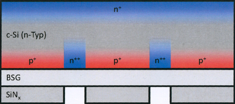
Scientists of the University of Konstanz have now developed a method for producing two differently n-doped areas and another p-doped area in a single-step diffusion process without the need for any additional masking and etching steps by using an n-type silicon substrate, for example.
To this end, only two layers have to be applied to the substrate, i.e. an one-sided borosilicate glass (BSG) layer covering the entire surface and a locally opened silicon nitride barrier layer.
During the subsequent POCl3 phosphorus diffusion in a furnace that is coated with suitable quantities of phosphorus, a lighter phosphorus doping (n+) is produced, for example for passivating the front side. At the same time, boron doping (p+, e.g. as emitter) is produced in the area that is covered by the BSG layer and the barrier layer. A more strongly doped phosphorus layer (n++) is created in the area that is only covered by the BSG layer.
As a result, no more than one high-temperature step is required to create the structure of a crystalline silicon rear contact solar cell with a passivated rear emitter.

